

NTU Opening Ceremony: “Where Creativity and Dreams Take Flight”
瀏覽器版本過舊,或未開啟 javascript
請更新瀏覽器或啟用 javascript
Spotlights
Date: May 11, 2023
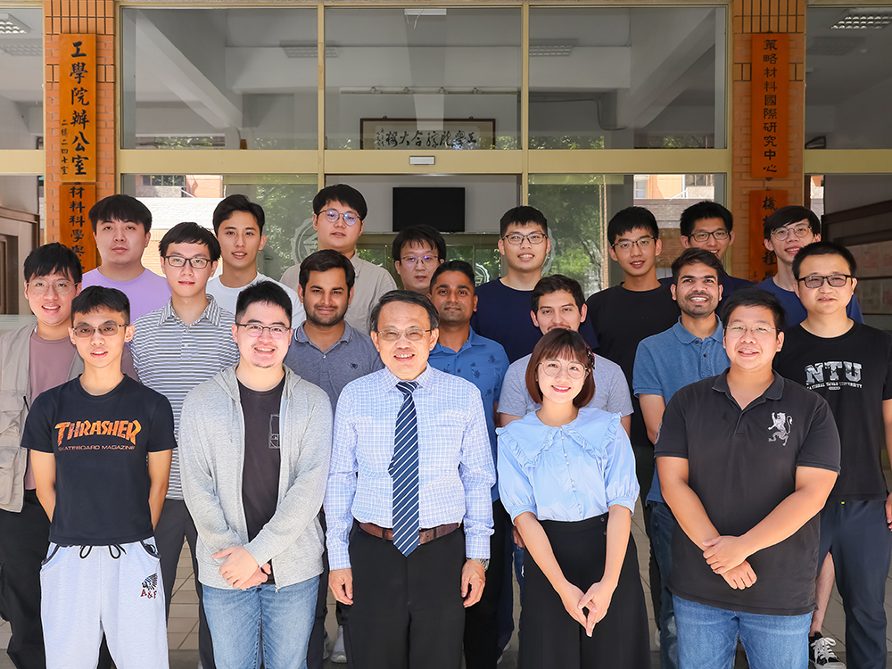
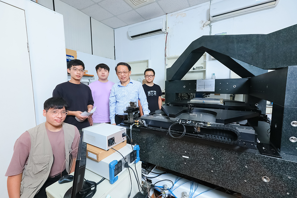
Group photo of Prof. Liang-Chia Chen and his research team.
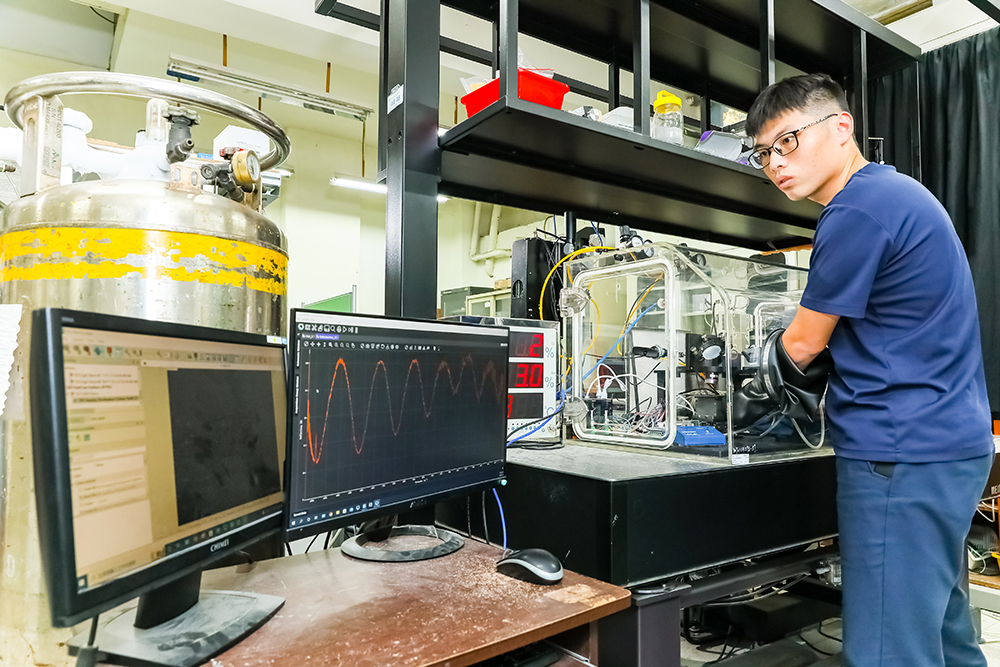
The deep UV measurement module developed by the team.
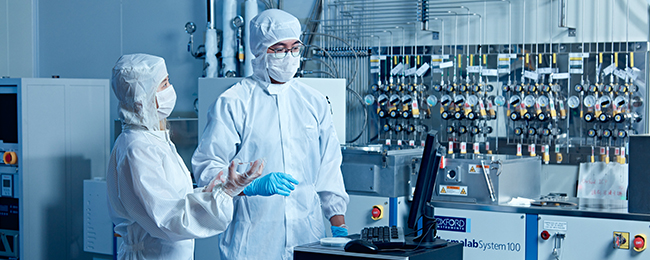
The high-precision measurement equipment developed by the team.
The National Science and Technology Council (NSTC) has founded a cross-disciplinary research team, led by Professor Liang-Chia Chen (陳亮嘉) of NTU's Department of Mechanical Engineering, to integrate cutting-edge technologies such as automated optical inspection (AOI), high-precision measurement, novel optical instrumentation, and AI algorithms. The result is the development of next-gen AOI systems that meet advanced manufacturing and semiconductor needs. The NSTC has also established the NTU Alliance for AOI Equipment R&D Coalition for Advanced manufacturing processes (AOIEC), composed of academic labs, equipment makers, and users, with 43 member companies, to advance AOI technology in the region.
The AOIEC is a specialized R&D organization focused on developing inline AOI equipment for advanced automated optical inspection and precision engineering industries. It brings together research teams from universities, including NTU, NYCU, NTUST, and NTUT, and collaborates with top-tier semiconductor vendors and Taiwan AOI makers, such as Chroma ATE, Gallant Precision Machining, Tri Technology, and Young Optics, to form a dedicated R&D taskforce. The goal is to develop AI-powered cutting-edge AOI technologies to fill critical technological gaps in optical critical dimension (OCD) metrology for 3D advanced packaging. The system can measure opening sizes down to submicron and has a depth-to-width ratio of 15 times, setting a new technology breakthrough for advanced semiconductor packaging technology. It was awarded the 2022 NSTC Future Technology Award for its achievement.
Semiconductor industry requires breakthroughs to close technology gaps and maintain global competitiveness
Taiwan's semiconductor industry plays a crucial role in the nation's economy and global competitiveness, driving advancements in technology through Moore's Law. The miniaturization of ICs and advancements in 3-D packaging technology bring benefits such as shorter conductor lengths, improved thermal conduction, higher signal bandwidth, lower power consumption, and smaller package volumes, yet also present measurement challenges. The critical dimension measurement of through silicon vias (TSVs) in 3-D packaging and 3-D ICs is challenging due to their small size and high depth-to-width ratio. These CDs directly impact electrical conductivity and process quality, yet current measurement techniques lack simultaneous accuracy and efficiency. The increasing depth-to-width ratio of submicron holes is a key technical issue in the global semiconductor competition, and the development of autonomous measurement technology and equipment is crucial for Taiwan's advancement in this field. According to SEMI's forecast, the demand for advanced measurement technology will continue to increase over the next five years.
Innovative Optical Technology Development to Break Measurement Bottleneck
Silicon vias are a crucial technology in advanced 3D packaging for vertical chip integration. However, as the size of silicon vias decreases and the depth-to-width ratio increases, effective measurement methods become scarce. The industry primarily relies on scanning electron microscopes (SEM) for cross-sectional critical dimension measurement, but this method is destructive and time-consuming. Atomic force microscopy has the potential for profile scanning but is inefficient and limited in accessing the hole interior. To address these challenges, we propose an innovative AI-powered optical measurement technology. Our solution uses physical optical simulation and AI deep learning optimization to penetrate high-depth-ratio blind holes and quickly detect precise critical dimension information, meeting strict inline process time demands.
The developed AI-powered optical measurement technology is based on advanced reflectometry and scatterometry. It uses novel numerical-controlled laser broadband light illumination for optical detection and AI deep learning optimization of inverse reasoning through innovative algorithms. It has overcome the technical barriers of minimum measurable aperture and maximum measurable depth-to-width ratio. The technology has been developed into several innovative optical critical dimension (OCD) measurement systems and techniques, capable of measuring world-leading micron-level silicon via critical dimensions with industrial verified results. The system can measure multiple critical dimension information in real time, with a signal-to-noise ratio (SNR) 28 times higher than non-coherent light sources, a world record achievement. This technology is currently world-leading and can be applied to many challenging measuring scenarios. A Taiwan invention patent (No. 111106641) and a US patent (No. 06A-210153US) have been filed for this development. The technology is also being developed in collaboration with equipment manufacturers and has received technology transfer and further research cooperation from several domestic AOI equipment manufacturers.
Technological transfer and industry validation for complete product and technology implementation
The dedicated R&D team from the AOIEC has successfully developed breakthrough measurement technologies and systems. Currently, our technology has been continuously validated by First tier semiconductor companies in Taiwan and has received continuing industry-academia collaboration and technology transfer from our cooperative AOI makers. Critical dimensions are validated through industrial samples, achieving sub-micron openings and a depth-to-width ratio of 15 times, leading the world's advanced semiconductor packaging technology. The developed deep UV measurement module will be further integrated and tested with the ultra-precision wafer measurement platform for Alva Test validation. The breakthrough in key technology will bring strong competitiveness to Taiwan's semiconductor industry and strengthen Taiwan's unique position in the world's semiconductor industry.
NTU Opening Ceremony: “Where Creativity and Dreams Take Flight”
Prof. Wei-Shiung Yang wins MOE National Excellent Teacher Award

NTU College of Public Health's Global Health Program Joins the Association of Schools of Public Health in the European Region
NTU hosts a successful dg.o 2024
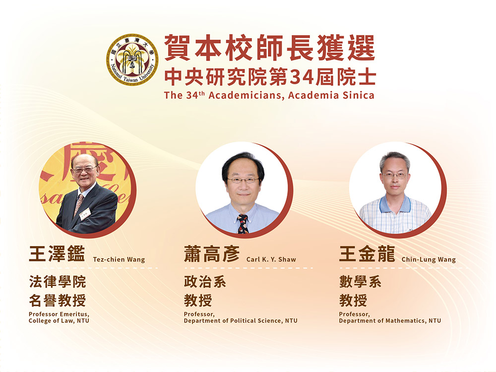
Congratulations to NTU faculty members elected as 34th AS academicians
Current Spotlights
NTU Opening Ceremony: “Where Creativity and Dreams Take Flight”
Prof. Wei-Shiung Yang wins MOE National Excellent Teacher Award
NTU College of Public Health's Global Health Program Joins the Association of Schools of Public Health in the European Region
NTU hosts a successful dg.o 2024
Congratulations to NTU faculty members elected as 34th AS academicians